
Peppered across rooftops, large solid-state solar panels can be seen while driving through virtually any neighborhood in the United States. However, as any of their owners will tell you, the cost is often high for the power benefits these systems provide. The reason is that the current standard single-junction silicon-based cells are approaching their theoretical limits of efficiency, and the multitude of costs associated with their application can be restrictive. Addressing these problems is one of the goals of Light-Material Interactions in Energy Conversion (LMI) Center.
The most common form of photovoltaic modules for the generation of electricity is based on silicon or similar solid-state semiconductor materials in single-junction cells. Single junction means that as light hits the semiconductor, only narrow ranges of light wavelengths are converted into electricity. The active wavelengths represent only a small percentage of the available solar spectrum. Even in ideal single-junction cells, there is a maximum efficiency of about 25 percent of only that narrow wavelength range, with commercial cells operating at about half of that efficiency.
Multi-junction cells can overcome these intrinsic limitations. By combining a variety of materials that each absorb specific wavelengths, these cells can absorb a larger net amount of the solar spectrum. However, combining each of these materials into a device by either wiring them, directly fusing them, or even gluing them together introduces losses in efficiency with added manufacturing costs.
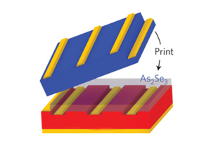
To combine multiple absorbing materials while avoiding issues of efficiency loss through previous bonding techniques, Xing Sheng and coworkers at the LMI labs at the University of Illinois, Urbana-Champaign have used a new type of bonding material in combination with well-known semiconductor printing techniques that generate test-sized microcells.
The process starts with synthesizing a well-known triple-junction semiconductor made by layering three different materials: InGaP, GaAs, and InGaAsNSb. These materials may bond directly on top of each other, and their molecular structures each match at their interfaces, a rare feature when trying to combine individual semiconductors. Separately, a common germanium-based semiconductor is dispersed on a conductive surface. The germanium base-layer is then coated with a novel As2Se3 glass, and the preformed triple-junction layer is then placed on top of the glass. The solar cell is then sealed to prevent further chemical reactions, and is wired to electrical contacts using methods similar to those used to wire microchips.
Under controlled illumination equivalent to our sun, the test cell demonstrates an efficiency of 32.9 percent. However, under concentrated light equivalent to about 1,000 suns, this efficiency peaks at 43.9 percent, nearly double the theoretical limit of a single-junction cell. The increase in efficiency over single-junction cells arises from the large spectrum light that can be absorbed by the assembly, from high-energy ultraviolet to low-energy, near-infrared light.
While other cutting-edge multi-junction cells have efficiencies approaching 45 percent, these systems require synthetic methods that are currently not scalable. The ability of the As2Se3 glass to join multiple semiconductor layers while dispersing heat and electrically insulating the layers without disturbing the light transmission throughout the assembly is the key breakthrough in this device. Additionally, the deposition of this glass layer is simple and controllable. The scientists note that this method may allow for larger stacks of semiconductors that could lead to efficiencies above 45 percent.
This work is far from complete. In addition to more junctions, "We are currently working on new materials for bottom junctions that will further increase the performance," said John Rogers, an LMI researcher at the University of Illinois, Urbana-Champaign and lead author on the paper. Scott Boroughs, another lead author and industrial collaborator from Semprius remarks, "Our technology, which enables the mechanical stacking of multi-junction microcells, has the potential to demonstrate a solar cell efficiency of >50 percent within the next several years."