

If we blew up an atom about a quarter million times, it would be the size of a golf ball! That’s how small an atom is. Researchers, however, have made it possible to work with materials that are as thick as one or just a few atoms. These materials are called 2D (two-dimensional) materials because effectively one of their dimensions is really small. Two-dimensional materials have been of increasing interest, because of their unusual characteristics and interesting properties such as exceptional strength and flexibility, and good thermal and electrical conductivity. These properties make them popular in a wide range of applications, including nanoelectronics for devices such as computers and cell phones, and clean energy technologies such as solar cells.
The use of 2D materials in clean energy technologies has been one of the research interests of the Center for Computational Design of Functional Layered Materials (CCDM), an Energy Frontier Research Center at Temple University. Some of the latest findings of Liping Yu, Adrienn Ruzsinszky, and John Perdew on 2D materials research connect the mechanical bending of the materials to their electrical properties by using first principles calculations. First principles methods are based on fundamental physics laws and provide detailed information of the mechanical, optical, and electrical properties of materials. Starting from the atomic structure and with description of the motion and interaction of subatomic particles, the physical and chemical properties of the materials can be determined, without making any assumptions.
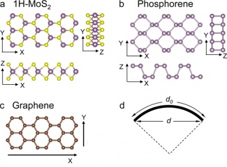
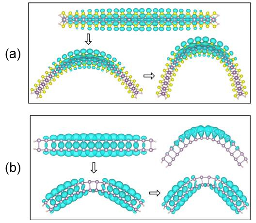
This research team, uses electronic structure calculations to relate mechanical properties, such as stress and bending energy, to the electrical properties of the material. They study the bending effects in nanoribbons of a single atomic layer, two-atomic layer, and three-atomic layer materials: graphene, phosphorene, and molybdenum disulfide, respectively. Their findings show that in molybdenum disulfide and phosphorene, bending can affect the distribution of the charges in the materials, causing charge localization. The charge localization can be controlled; therefore, the conductivity of molybdenum disulfide and phosphorene can be altered or turned on and off. Conversely, there seems to be no such effect of bending in graphene, thus making it a suitable material for applications where flexibility without other property change is required.
The researchers provide fundamental details for understanding the correlation of the properties of 2D materials, which opens the way to further technological development. The team’s results suggest that it’s possible to control the physical properties of 2D materials by mechanical bending and assist in new material design.
The researchers show that manipulating the electrical properties by applying mechanical stress and strain is possible, while they also emphasize the importance of computational methods in new material development and design and technological development.
