
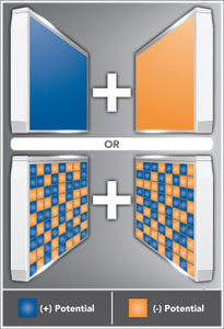
Scientists at the Non-equilibrium Energy Research Center, NERC, are challenging the conventional view of how static electricity exchanges between materials when brought into contact. They show that polymer surfaces possess a mosaic of static charge domains with positive and negative regions as opposed to a uniform surface of just one charge type. The work, led by Bartosz Grzybowski at Northwestern University and director of the NERC, was published in Science.
Examples of static charge buildup and discharge are all around us ranging from “static cling” when laundry is taken out of the dryer to lightning flashes during a storm. Static electricity is already used in commercial applications such as photocopying and laser printing. However, the insights of this work could enable the development of devices that store static charge and convert the electrical potential into useful forms of energy.
Contact electrification occurs when static charge is transferred between two insulating surfaces that are brought into contact and then separated. Generally, it was believed that the one of the materials develops a uniformly positive charge and the other, a uniformly negative charge. The NERC scientists used Kelvin force microscopy, or KFM, to study contact electrified polymer surfaces, where an atomically sharp conductive probe tip is scanned over the polymer and the potential offset between the tip and surface is measured at each point. This technique enabled the researchers to zoom in and image the surface charge potential with nanometer resolution (1 nanometer is about 100,000 times smaller than the diameter of a human hair).
While indeed the net charge of one of the polymers is positive and the other negative, the KFM images reveal that both surfaces display a mosaic pattern of positively and negatively charged regions that are only hundreds of nanometers in size. This means the charge density within any one of the nanoscale domains is about 100x greater than the net charge that would be measured over the entire surface.
“Knowing there is 100 times more static charge than ever previously measured turns our attention to this ‘hidden’ source of electrical energy,” said Bilge Baytekin, co-author of the article. “We would like to focus more on converting this electrical energy into chemical energy.”
The discovery demonstrates that the ability to probe material properties on the nanoscale can provide new insights and potential uses for everyday phenomena. In the future, one can imagine devices that capture the ambient static electricity that is normally wasted and use the highly charged surfaces to provide portable lighting or drive industrially important chemical reactions.