
Collaboration between two Energy Frontier Research Centers has produced the first 3D photonic crystal, a material designed to control the propagation of light, incorporated into an electronically addressable device. The research was a joint effort between the Light-Material Interactions in Energy Conversion EFRC and the Center for Energy Nanoscience.
“This work was conceived to address a long-standing problem in 3D photonic crystals,” says Paul Braun of the Light-Material Interactions in Energy Conversion Center and professor at the University of Illinois at Urbana-Champaign. “Our demonstration of optoelectronically active 3D photonic crystals provides motivation for thinking seriously of designing structures for specific applications.”
Envisioned applications include cloaking devices, high-efficiency lasers, light-emitting diodes (LEDs) and solar cells.
The arrangement of atoms in a solid determines its electronic properties. For example, semiconductors are materials in between insulators and conductors whose electrical conductivity can be precisely tuned by adding small amounts of impurity atoms to the atomic crystal. The electronic transistor, a device that controls the flow of electrical current through a semiconductor, has become a ubiquitous element in modern electronics, including computers, televisions and cell phones.
Now zoom out from the atomic level to the microscale, where 1 micrometer is about 10,000 times larger than an atom, but still 100 times smaller than the width of a human hair. Photonic crystals possessing a periodic, or regularly repeating, structure on the microscale can be used to manipulate the flow of photons, the quantized units of light. Naturally occurring photonic crystals include butterfly wings, peacock feathers and oyster shells, whose periodic microstructure is responsible for their iridescent sheen. The design of synthetic photonic materials to guide the propagation of light through high-quality semiconductors is a crucial step towards producing the novel optoelectronic devices mentioned above.
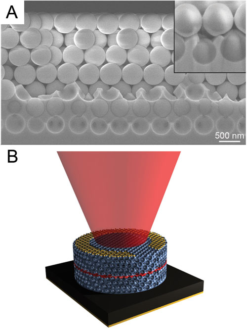
The difficulty in coupling photonic and electronic materials is that it requires near perfect ordering of the material on two very different length scales, both the atomic and microscale. The EFRC researchers overcame this obstacle by performing selective area growth of the semiconductor material, gallium arsenide (GaAs), through a 3D structured template. Gaseous precursors, that are normally deposited on a planar surface to form a film of GaAs, instead flowed through a porous template consisting of a well-ordered array of silica microspheres (imagine a box of ping-pong balls). The precursor gases flowed through the void spaces between the microspheres and only deposited on the bottom surface, building up the GaAs crystal in between the spheres. See Figure A. This produced a 3D structure with crystalline atomic order and a periodic array of micropores after removal of the template.
To fabricate an LED device from the 3D photonic crystal, the researchers alternated the vapor precursors to build up layers of GaAs and indium gallium arsenide. See Figure B. When electrical current is passed through the device, light is emitted from the structure, which is the first example of an electrically pumped 3D photonic crystal device.
While electronic-photonic coupling in the LED is preliminary, it offers a look into a possible future. "We can now begin to think about the design of structures which optimize both the optical and electronic properties of the resultant material to enable a new class of devices for solid-state lighting and photovoltaics,” says Erik Nelson, a member of the EFRC team.