
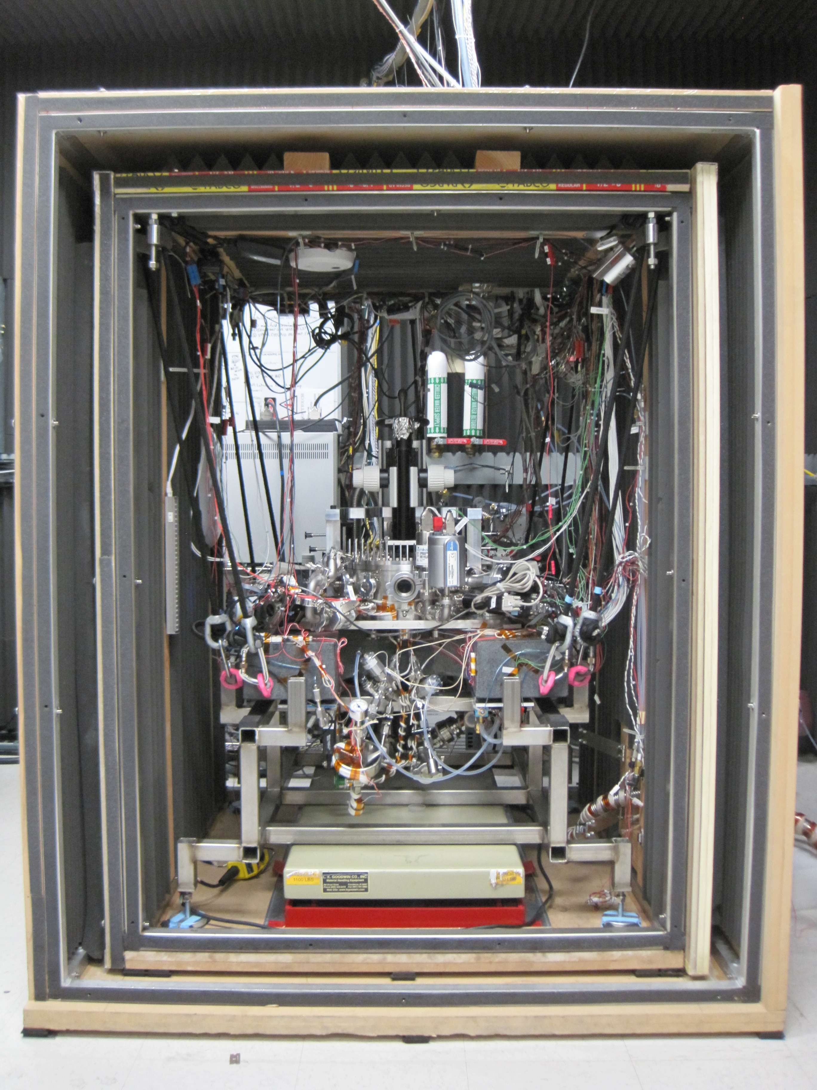
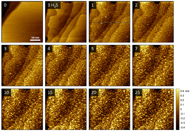
An artist that carves a statue constantly scans the surface of his creation with his eyes to decide where to place his chisel next. It follows that one should be able to measure similarly the progress of a manufacturing or, more generally, “shaping” process. Unfortunately, at the atomic scale, it is not that simple. Nano-devices are being prepared blindly and then taken to a different location where they can be measured and characterized. Given how sensitive these devices are to environmental conditions, this process is far from ideal. In addition, little can be said about the critical parameters of the manufacturing process that affect the properties of the sample. To circumvent this problem, scientists at the Center on Nanostructuring for Efficient Energy Conversion (CNEEC) built an apparatus that can measure, or “see,” the deposition progress of nanometer-thick layers.
Nanoscale structures and devices are instrumental in enabling a number of renewable energy technologies. Examples include solar cells, catalysts for fuel conversion using sunlight and fuel cells. As in the macro-world, uniformity and manufacturing tolerances strongly affect the efficient operation of these devices; for example, comparing a regular chair to one whose legs vary in height by a few inches. Hence, controlled nano-manufacturing processes are paramount in the rising sector of nanotechnology.
Combining Technologies Provides Tailored Surfaces and Crisp Views: Atomic layer deposition (ALD) is a manufacturing method used by scientists to make atomically thick layers. The process works in cycles. It starts by injecting a chemical vapor or precursor into a chamber where it reacts with an activated surface. The reaction is self-limiting, meaning that after an atomically thick layer is formed, it stops. The chemical is purged and another precursor is injected that will reactivate the surface and prepare it for deposition of the next layer. The process is repeated until a thick-enough layer is obtained.
Scanning tunneling microscopy (STM) works by bringing an atomically sharp conducting tip close to (but not touching) the surface of the sample. By applying a voltage across the tip and sample, electrons jump across by a quantum mechanical effect called “tunneling.” As expected, the degree of tunneling depends on the distance of the tip from the sample surface and on the surface’s electrical properties. By scanning the tip along the sample surface, scientists obtain local information; for example, surface height and electrical conductivity. STM technology has improved significantly lately, making it possible to identify individual atoms.
First-Ever Use of ALD with STM: Combining ALD with STM is inherently difficult. STM is ideally performed at low temperatures and high vacuum to limit collisions of atoms from the environment with the sensitive STM tip. In contrast, ALD requires elevated temperatures to allow the reactions to proceed, while the injection of chemical vapors obviously contradicts having a vacuum. Nevertheless, through complex engineering, the scientists built a custom experimental setup that allowed them to demonstrate the first in situ nanometer-scale topographical observations of ALD by using STM. Their findings are expected to lead to a better understanding of the parameters that affect film growth in ALD and hence help optimize the manufacturing processes for nanoscale devices.