
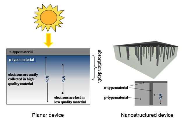
Imagine reducing time to model materials systems by a factor of 1000 or more. Remarkably, researchers with the Center on Nanostructuring for Efficient Energy Conversion did just that by developing a novel analytical method. The team used this method to compare solar cell energy conversion efficiencies for various material structures.
The lure of solar cell technology, aka photovoltaics, stems from the promise of a limitless and environmentally friendly source of electricity; coupled with the ever-increasing demand for energy, photovoltaics are receiving increased research attention. In photovoltaic devices, creation of an electric current occurs when solar radiation, that is, photons, excite electrons at a p-n (positive-negative) junction. The junction acts as a two-way road, allowing photo-excited charges to flow in opposite directions, leading to an electric current.
Existing theoretical studies do not fully account for the three-dimensional behavior of solar cell devices, due to the computational resources necessary to integrate mathematical models. “When we [the research group] tried to do the simulations numerically on an 8-core processor, it would take up to 3 days for each data point,” said Artit Wangperawong, lead researcher on the study. “We then took an analytical approach to the three-dimensional problem, which allowed us to produce a data point in less than a minute on a single core.”
The team used the novel analytical method to demonstrate that interdigitated (visualize interlocking fingers of two clasped hands) junctions can offer superior energy conversion performance over planar geometries and isolated junctions. For example, in interdigitated junction modeling, multiple p-n interfaces are simulated, which allow photo-generated charges to diffuse to any nearby junction. Isolated junction modeling accounts for one primary charge diffusion path, which does not accurately reflect three-dimensional behavior.
The group’s time-saving modeling technique has enormous potential in modeling nano-structured geometries and materials systems, as well as systems beyond photovoltaics. While a commercially available simulation tool is a distant goal, Artit says, further developments may be forthcoming with continued research.